Chips inside of computers, mobile phones and any other complex electronic gadgets, consists of billions or at least millions of transistors in nowadays. Despite this, engineers are looking forward to pack more and more transistors in chip wafers to reach better performance. However, conventional MOSFETs inside of chips, which are silicon based transistors have already reached their limits in scaling. Further scaling of silicon based transistors, will lead to issues such as current leakage and short channel effects. Subsequently, this will lead to catastrophic issues in very large scale integrations. The carbon nanotube based field effect transistors are perfect candidates to replace MOSFETS. Due to their unique electronic and mechanical material properties, CNTFETs may overcome the bottlenecks of MOSFETs in scaling. Therefore, we have investigated different compact models for circuit analysis and highlighted pros and cons of each models. In addition, various analog and digital circuit application were simulated using nano scale dimensions. The results yields that, CNTFET’s performance is superior compared to conventional silicon based MOSFETS, showing ultra-low power consumption and/or high frequency responses. January 2021.
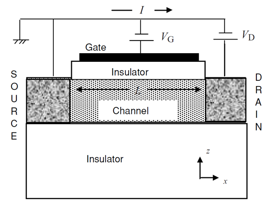
Simple Nano-Transistor
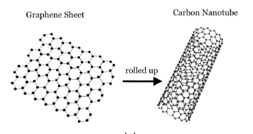
Carbon Nanotube
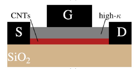
CNTFET
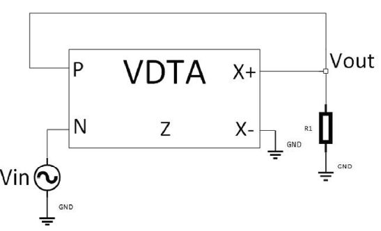
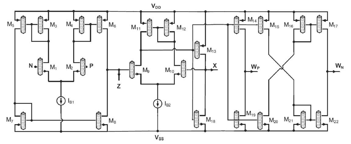
Analog application circuits of CNTFET are demonstrated below. Simulations were perfermed with SPICE tools.
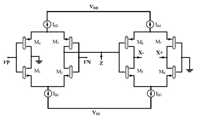
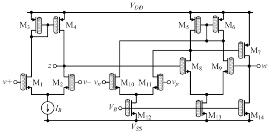
VDTA CNTFET Circuit
VDTA CNTFET Schmitt Circuit
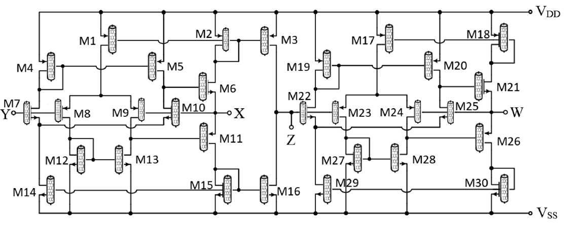
CFOA CNTFET Schmitt Circuit
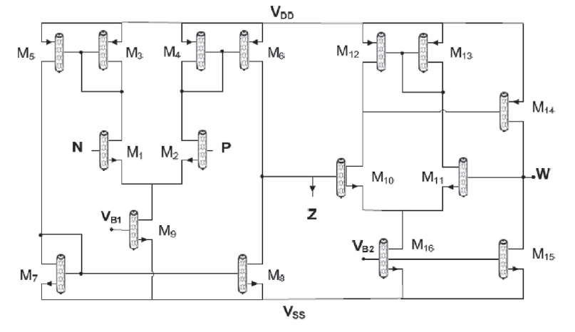
VDBA CNTFET Schmitt Circuit
VDCC CNTFET Schmitt Circuit